


Expectations
The researcher has already completed the verification of the principle of each component and is now proceeding with demonstrations using prototypes. We aim to commercialize this technology through joint research with companies, while also obtaining grants in the future. We are seeking companies (especially those with semiconductor laser manufacturing technology) interested in developing a completely new, high-efficiency terahertz-wave semiconductor laser capable of operating at high temperatures above room temperature, utilizing this technology.
Advantage and Core Benefit
- Solves the problems of quantum cascade lasers, such as the need for wavelength conversion for high temperature operation and energy loss when electrons are converted to light.
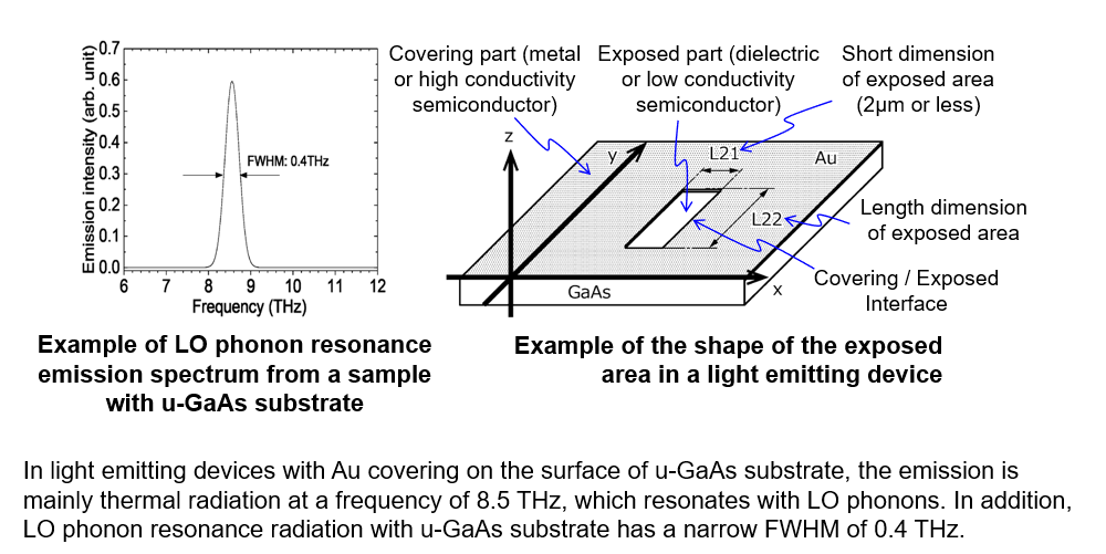
- Simple structure with a short dimension of 2 µm or less on the dielectric substrate surface exposed between the covering portions of the conductor, capable of emitting longitudinal optical (LO) phonon resonance light from the exposed portions by current injection.
- The wavelength is object-specific, fluctuates little and is variable with the choice of material. Average output power is expected to be several hundred mW.
- Significantly reduced blackbody radiation background noise, faster conversion rate to light, single photon emission, and improved spectral controllability.
Technology Overview & Background
Electromagnetic waves in the terahertz wave range are expected to have a variety of applications. For example, they are expected to realize ultra-high-capacity communications over short distances, non-destructive and non-contact inspection and analysis of living organisms and chemical materials, and observation of signals flying from space. However, conventional quantum cascade lasers, in principle, require wavelength conversion for high-temperature operation, and energy leakage to lattice vibrations occurs when electrons are converted to light.
This technology is a light emitting device for semiconductor lasers in the terahertz wave region that solves these problems in principle. Unlike conventional light emitting devices that convert electron energy into electromagnetic waves, this technology directly converts phonon energy, which is converted from electrons at high speed, into electromagnetic waves. Therefore, it can operate at high temperatures and has extremely high energy usage efficiency.
As shown in the figure, it has a simple structure with a short dimension of 2 µm or less on the dielectric substrate surface exposed between the covering portions of the conductor, and can emit LO phonon resonance light from the exposed area by current injection. The wavelength is object-specific, fluctuates little and is variable with the choice of material. The average output is expected to be in the range of several to several hundred mW. It also greatly reduces blackbody radiation background noise, enabling fast conversion to light and single photon emission.
 |
Patents
PCT/JP2024/018344 (pending)
Principal Researcher & Academic Institution
Yoshihiro Ishitani
(Chiba University, Graduate School of Engineering, Professor)
Project No.HK-04780b