


Summary
- Proposes a new concept of using electric charge from etch plasma used in semiconductor device fabrication as a power source to drive small-scale circuits during device fabrication.
- Showing a physical unclonable functions (PUFs) application using our technology. The PUFs fabricated during etching process are inseparable and reliable.
- Proven technology by fabricating chips in the CMOS process. Successfully generated PUF with sufficient entropy using etch plasma as a power source.
- Other applications such as device quality checks and calibration for problem detection are welcome.
Background & Technology
Professor Noriyuki Miura of Osaka University’s Graduate School of Information Science and Technology proposes a new technology that uses etch plasma as an untapped source of power for the semiconductor device manufacturing process.
The core of this technology is the use of “antennas” pre-formed on dicing streets on semiconductor wafers to collect etch plasma (Figure 1). The plasma charges collected by the antenna drive circuits placed on the dicing street and inside the semiconductor chip. Professor Miura and his colleagues call these circuits “Fetal Movement Circuits,” meaning that they are driven during device fabrication.
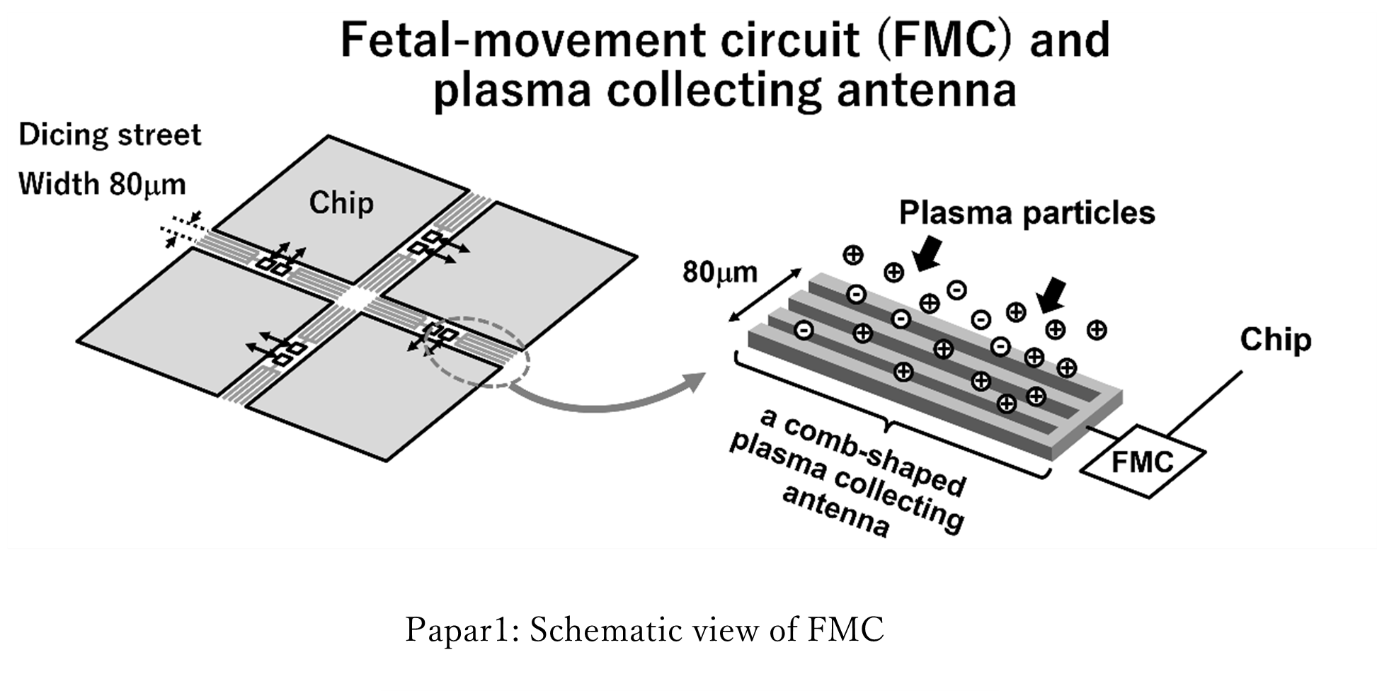 |
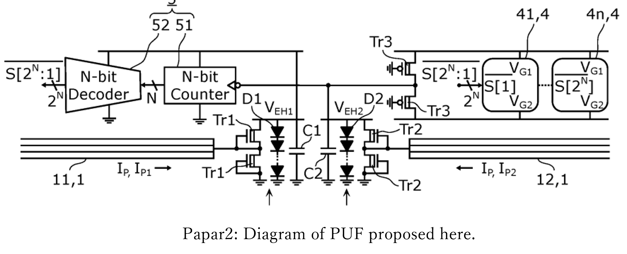
FMCs have a variety of possible applications. As an example of an FMC, Prof. Miura and his colleagues have devised a physical unclonable function (PUF). The invented PUF consists of a plasma collection antenna, a boost circuit, a group of transistors that are the main body of the PUF, and a driving circuit for generating the PUF (Figure 2). The transistor group (S[1] to S[2N] in the figure) is a collection of transistor pairs, each pair consisting of two transistors connected in parallel. First, a power supply voltage based on the plasma charge collected by the antenna is applied to this group of transistors through the drive circuit (counter and decoder on the left in the figure). Then, for each transistor pair, the transistor with the lowest withstand voltage (i.e., with the weakest gate oxide film) is destroyed first, and this occurs in all transistor pairs. Which of the transistor pairs is destroyed first is completely random and cannot be reproduced. The group of transistors that survives the breakdown thus becomes the PUF. When the chip is used, the PUF response is obtained by reading out the breakdown pattern of this PUF.
 |
This technology is characterized by two features: high security in that the PUF cannot be physically separated from the device, and the cost advantage of using a previously discarded energy source. Since the PUFs in this technology are generated in parallel with the manufacturing of the semiconductor device, they are embedded in the device and can only be separated by destroying the device. While some conventional PUFs can be separated from the device, the PUFs of this technology are considered to be more secure. In addition, since the creation of PUFs of this technology does not require an external power supply, the cost of hardware modification of device manufacturing equipment can be reduced, and changes to the manufacturing process can also be kept to a minimum. In addition, there is little cost increase in terms of energy, as it is not an addition to the conventional process.
The application of FMC technology is not limited to PUFs. For example, this technology can be used to create quality control functions such as monitoring the amount of etching plasma in the semiconductor manufacturing process and calibrating chips to reflect quality inspections and testing of chips in production.
In addition, various other applications are possible, such as the creation of PUFs based on principles other than those described above.
Data
Prof. Miura and his colleagues are in the process of demonstrating the operation of the PUF described in this article (see Reference 1).
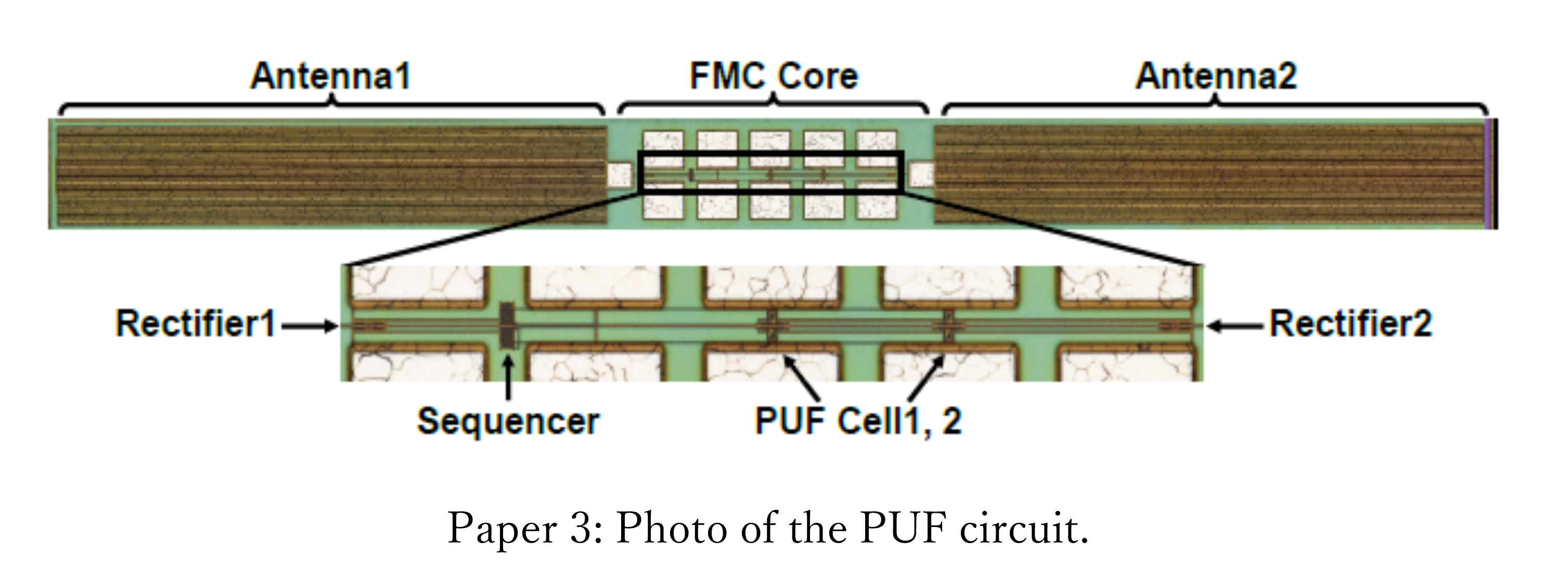
- For the technology demonstration, a test chip was fabricated using a 180nm CMOS process. The fabricated circuit (Figure 3) consists of an antenna, a control circuit, a PUF cell (a pair of transistors), and a voltage measurement terminal (white part in the figure). There are 230 PUF cells on one test chip.
- In the process of manufacturing the above circuit on the test chip, as expected, the FMC was driven by the etching plasma as an energy source and PUFs were created. After the test chip fabrication, the current of the internal transistor was measured for each PUF cell, and it was confirmed that one of the pairs was destroyed in all cells.
- The current values of all PUF cells were measured and a binary PUF response was created based on the high and low current values. The entropy of this response is approximately 0.5, which is sufficiently complex to be practical as a PUF.
 |
Expectation
We propose collaboration with companies interested in developing PUFs and semiconductor devices using this technology. We hope that you will utilize the PUF of this technology to improve the security of semiconductor devices developed by your company. In addition to PUF, the following applications are also envisioned.
- Quality testing of devices during manufacturing. Test circuits are driven by embryonic circuits. Potential to reduce costs and time costs associated with testing.
- Pre-configuration of chips. Based on the results of the above test, the operating conditions of a good circuit are calculated, and the parameters necessary for these conditions are written to non-volatile memory during manufacturing.
We ask that your company take the initiative in transferring this technology to your company. The University can assist you in the development of your company in the following ways
- Responding to questions (excluding confidential information)
- Meeting with the researcher to discuss the details
- Exchange of information under NDA
- Joint research
- Patent Licensing
Patent & Publication
- PCT applied WO/2024/157600
- Paper 1:Presentation material by Dr. Miura explaining this technology
A Fetal-Movement Circuit Harvesting High-Energy Plasma During Fabrication, Concept, and Its Application to Self-Programming PUF
https://ieeexplore.ieee.org/document/10247264
Project.DA-04488a