


Advantages
- Electronic circuits powered by etch plasma.
- Semiconductor quality inspection circuits, physical replication difficulty function (PUF) circuits, and other attached circuits on the semiconductor wafer are driven without an external power supply.
- PUF cell operation has been demonstrated using test chips fabricated in 180-nm standard CMOS.
Background & Technology
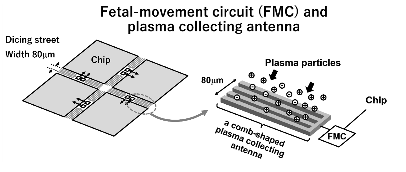
Etch plasma in the semiconductor manufacturing process is so energetic that it destroys and degrades the gate oxide film of transistors. Professor Noriyuki Miura of Osaka University’s Graduate School of Information Science and Technology proposes a semiconductor circuit that utilizes this plasma as an untapped source of electric power. The technology uses a comb-shaped antenna pattern formed in the dicing street, which must be inserted between semiconductor chips for the process, to drive circuits placed in the dicing street and semiconductor chips, hereinafter referred to as fetal movement circuits (FMC), using the current obtained by collecting etched plasma as a power source. The FMC is a circuit that is powered by the current obtained by etch plasma. For example, there are various possible applications of this technology, such as monitoring the amount of etch plasma in semiconductor manufacturing processes, quality control functions to determine the quality of chips during manufacturing and to calibrate chips, and writing physical unclonable functions (PUFs). Using this technology, special circuits as FMCs can be integrated into silicon wafers during the etching process without requiring extra silicon area, external power supplies to drive the circuits, and modifications to conventional semiconductor manufacturing processes.
Currently, the most advanced topic of research at Osaka University is the technique of writing physical unclonable functions (PUFs) using FMCs. Specifically, in a method to generate PUF authentication patterns by randomly destroying transistors in a chip by high voltage, the university’s technology supplies high voltage for transistor destruction from a plasma collecting antenna and power supply circuit constructed on the dicing street. Since the authentication pattern generated by this method is physically written, it is expected to be a highly accurate PUF with little instability when read. The researchers have already demonstrated the operation of the PUF cell in a preliminary evaluation using a test chip manufactured in 180nm standard CMOS.
 |
Expectation
We propose to collaborate with companies interested in developing technologies and products using this technology. The university has already processed an FMC on a semiconductor device and confirmed that it can be driven. We expect that companies will take the initiative in transferring this technology to their own technologies and products. The university can provide various types of assistance, such as providing scientific knowledge necessary for companies to develop the technology and consulting with them on development policies. Ultimately, the university can also ensure the exclusivity of the business by licensing the patents the university holds.
Patent & Publication
Patent pending in Japan. Osaka University plans to file a PCT application for this technology.
・Kotaro Naruse, Takayuki Ueda, Jun Shiomi, Yoshihiro Midoh, and Noriyuki Miura, “A Self-Programming PUF Harvesting the High-Energy Plasma During Fabrication,” International Solid-State Circuits Conference (ISSCC) Digest of Technical Papers, pp. 218-219, Feb. 2023.
Project No. DA-04488