


Advantages
- Highly functional KPFM with high frequency (>500 kHz) AC bias voltage applied to the probe.
- Enables ‘accurate’ measurement of level densities at material surfaces and interfaces. For example, the interfacial level density at semiconductor heterojunction interfaces can be measured without so-called band bending effects.
- Measurement technology that assists in the development of new materials and devices by enabling the precise evaluation of the surface state of various materials, such as wide-gap semiconductors, high-k gate dielectrics, graphene and battery electrodes.
Background & Technology
As devices become smaller and more sophisticated, more accurate methods of measuring the interface state are required, e.g., for observing the shape and properties of the junction interface in the design and manufacture of semiconductor devices and for product inspection, or for evaluating the properties of electrode surface states in the design of solar cells, fuel cells and lithium-ion batteries. However, conventional microscopes for measuring interface layer density, known as “conductive AFM,” have problems such as low measurement sensitivity and spatial and temporal resolution, as well as the influence of stray capacitance from the capacitance sensor in the device.
Prof. Sugarawa, The University of Osaka, had previously developed a technique to speed up the time resolution of contact potential measurements in KPFM (Kelvin Probe Force Microscopy) by up to 1000 times by using a high frequency applied AC bias voltage. In this study, the technology has been further developed and a mechanism has been developed to switch the applied AC bias between high and low frequency at high speed. Using this mechanism, it is now possible to measure the level density of the surface of the target object on the nanometer scale (see figure). This is how it works. With conventional technology, the AC bias that can be applied is limited to low frequencies. As a result, the measured information was a mixture of information from the bulk of the semiconductor and the band bending of the surface. However, this research has enabled the application of high frequency bias voltages and fast switching between low and high frequency voltages. As a result, the bulk and band-bending information of the semiconductor can now be separated. In other words, it is now possible to read the ‘true’ bulk information of the semiconductor. Prof. Sugawara and colleagues have created this KPFM, measured the change in electrostatic force on the surface of ion-implanted silicon when AC bias voltages of different frequencies are applied, and successfully observed the density of interfacial layers (see the paper as shown below).
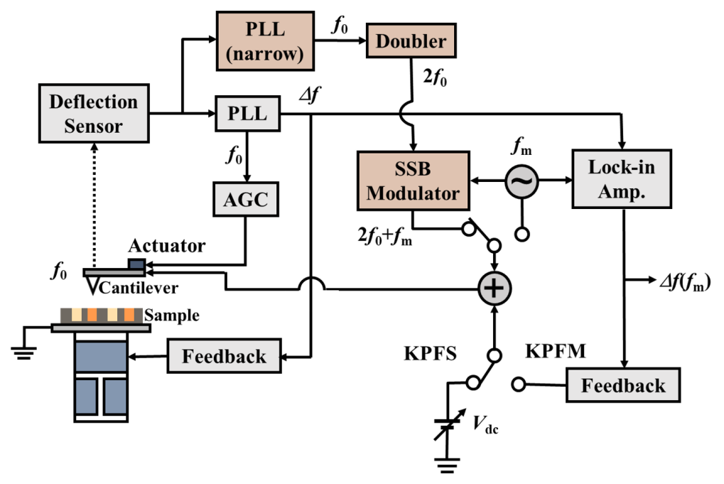 |
Figure 1. Circuit configuration of the KPFM of this technology. The switching unit in the center right of the diagram switches between high (2f0+fm) and low (fm) frequencies. (Adapted from a paper by Prof. Sugawara)
Researcher
Yasuhiro SUGAWARA, Professor, The University of Osaka Graduate School of Engineering
Patent & Publication
・Patent pending
・Beilstein J. Nanotechnol. 2023, 14, 175-189: Principles and experimental results are reported.
Expectation
The University of Osaka is looking for partner companies to develop microscopy equipment using this technology. The University also welcomes joint research with companies that have needs to measure interface level density, targeting semiconductor manufacturing and battery electrode production, etc.
Project No. DA-04297